One of the last steps in the PCB (printed circuit board) manufacturing process, which we have described to you on this page, is the application of surface finishes, the main objective of which is to ensure the best soldering of components during assembly.
We thought of this short in-depth study, divided into two specials, to support you in making a better choice at the design stage with the goal of optimizing the overall performance of your printed circuit board. Indeed, PCB surface finishing, which can be organic or metallic, affects PCB assembly and determines the reliability of the circuit board. The finishes mainly used in PCB manufacturing today are:
- Lead-Free HASL
- Electroless Nickel Immersion Gold (ENIG)
- Hard Gold (Electrolytic Nickel/Gold, Hard & Soft Au wire bondable)
- Electroless Nickel Electroless Palladium Immersion Gold (ENEPIG)
- Chemical Tin (Immersion Tin)
- Organic Solderability Preservative (OSP)
- Chemical Silver (Immersion Silver)
The choice of the correct surface finish is made based on many aspects, again referring to the IPC Guidelines for the type of components to be mounted on the board itself and the type of process used by the assembler (e.g., reflow and soldering modes). For example, for layouts with a large number of SMD components, it is recommended to choose a very planar surface finish such as ENIG. Or, chemical tin might be the right choice for special solderability requirements.
Different surface finishes have an impact on how the material is stored and on the time window of processability of PCBs after they are manufactured. For example, the shelf life of a PCB with Chemical Tin surface finish is half that of a PCB with Lead-free HASL finish.
The main features of the first three technologies listed above follow:
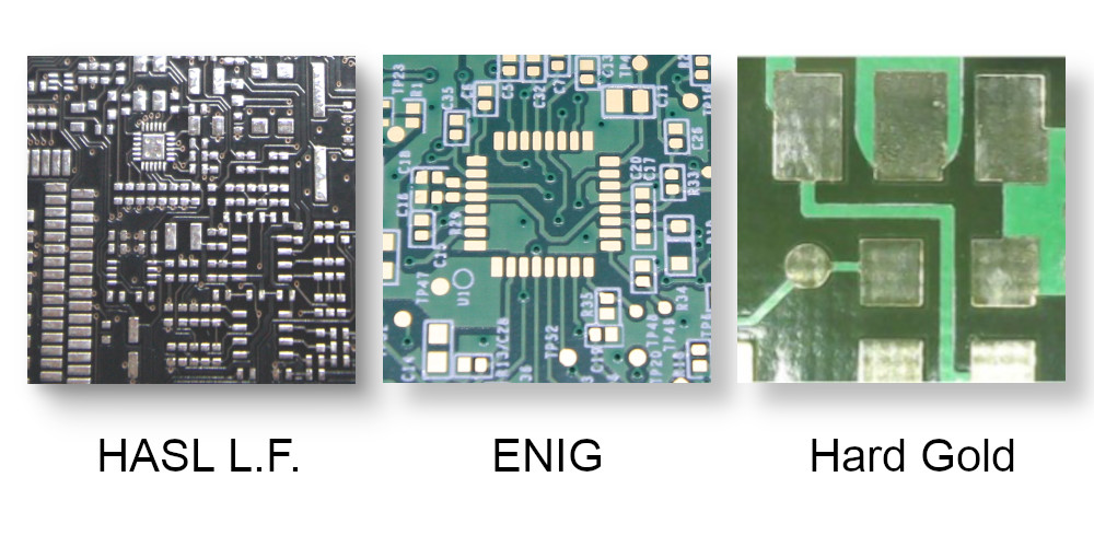
Lead-Free HASL
Among the most widely used finishes, standard for the entire industry, whose advantages are availability from essentially all manufacturers and low cost. Shelf life is among the longest, and reworkability is also optimal.
The downsides of this technology include poor flatness, and it is also not suitable for BGA (fine-pitch) applications and layouts involving isolation between the pins of the ICs (Solder Bridging). The process brings the boards to 265° which causes a major thermal shock to the board, which could also damage the internal interconnects. If the board provide for small-diameter holes, there is a risk of plugging them during the application of the finish itself.
Electroless Nickel Immersion Gold (ENIG)
ENIG is a coating composed of two layers, specifically 0.05-2 μm of Gold protecting 3-6 μm of Nickel. The advantages of this technology are surface flatness and good performance for Plated Through Holes (PTH). The shelf life is good and no Lead is used for greater environmental friendliness and safety.
Downsides include cost, which is higher than other solutions, also due to the complexity of the process. ENIG-treated boards are not reworkable. This finish tends to oxidize if not properly stored.
Hard Gold
Hard Gold or Electrolytic Gold consists of a layer of gold whose thickness can range from 0.8 to 1.25 μm (depending on Class) deposited on top of 2.5 μm of Nickel. It is particularly suitable for areas of high wear and tear (e.g., contact rubbing on the pins of a USB port). In addition to the tough and durable surface, the other pros of this solution are good shelf life and again Lead is not used.
The high cost of this solution stems not only from the cost of the material itself but also from the more complex machining process, which may include variations such as taping. This finish is not weldable for Au thicknesses above 0.4 μm (as per IPC guidelines) and is difficult to combine with other types of surface finish.
In the next special dedicated to surface finishings we will look in detail at the other finishes namely ENEPIG, Chemical Tin, OSP and Chemical Silver.