


The use of innovative substrates, such as PET, in the production of electronic boards offers significant advantages in terms of flexibility, light weight and reduced cost. These materials enable the fabrication of thinner, stronger circuits that are ideal for applications such as wearable devices, sensors and flexible electronics. In addition, its compatibility with additive printing techniques simplifies manufacturing, reducing environmental impact. These substrates represent the future of electronics, combining high performance with sustainability.
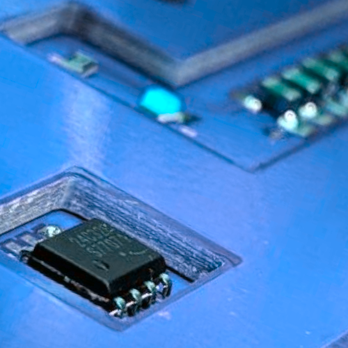
Another very innovative and high-performance technology, particularly suited to markets such as telecommunications and medical, is Embedded PCBs: printed circuit boards that integrate electronic components, such as resistors, capacitors, or integrated circuits, directly within the substrate instead of surface-mounting them. This approach reduces board size, improves electrical performance through shorter signal paths, and increases reliability by eliminating soldered connections prone to failure.
Polyethylene terephthalate
FR4 or advanced composite materials
Teflon and FR4 PCB
PCB in FR4
Finished through-hole minimum diameter 100 µm Aspect Ratio PTH = 1:6 or 1:10
Microvia minimum diameter 75 µm (laser drilling) Aspect Ratio blind hole = 1
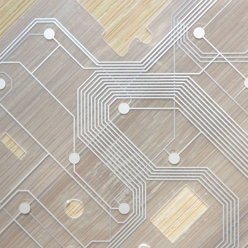
Fine line minimum track/insulation width 50 µm tolerance ±10%
Minimum Kapton thickness 50 µm, 25 µm on request
SolderMask/SolderDam glazing or screen printing 100 µm standard and 70 µm on request
Maximum PCB thickness 6.5 mm
Dettagli di contatto
Contact details