
full support
A full range of services to support your creations

We know that the PCB design process could be complicated. Our experienced CAM engineers can help you: we will guide you through every step, from masterization to industrialization, achieving the most reliable and cost-effective design solution.
The goal is to provide advice aimed at improving, when possible, mass production, optimizing material use (minimizing waste) and refining the production process in order to avoid critical issues that generate waste and production delays.


Collaborating with the top global players in the shipping market, we are able to provide international services by sea, air and land aiming at the best ratio of cost and speed, organizing possible groupage to optimize the expense. In order to avoid even the slightest degradation in the condition of PCBs, special care is taken in packaging. In fact, there are silica gel and moisture indicator in the individual packages, and on the outside there is an adhesive label indicating product code, quantity and date code. This information will be replicated on the outer box, ensuring constant tracking of shipments

Our customer support and sales team are always at your disposal, ensuring professional advice and in many cases interesting insights into the development of your project. In fact, together with the client we try to create a service that takes into account all needs on a case-by-case basis, providing unique solutions according to each individual request. Usually requests for quotation are processed in maximum 24-36h to allow the client to have as immediate an understanding as possible of the costs to be incurred in order to calmly and carefully plan the best production and purchasing strategies.
Pcb manufacturing
Our workflow

Design review and engineering support
- As the first step Tekube receives the design files directly from the client. The data package includes distinct information of the layers, silk screen printing, solder mask, drilling point and other details. The most common extension used for these products are Extended Gerber and ODB++. Thanks to CAD/CAM stations, exporting is always possible, .dwg included.
- After having received the Gerber files, the Tekube technical department starts, in agreement with the client, a review phase of the data package: included information will have to be in compliance with manufacturers capabilities and also IPC A600_G provisions.
- The technical department, thanks to the experience achieved in the years, is usually able to suggest engineering enhancements to allow for a more efficient industrialization.
- Having considered the peculiarities of the product, the best production partner is selected, basing the choice on criteria such as technical fitness (capabilities) and business terms. This tasks usually takes less than 24 hours, allowing the client to receive a quotation in shortest time possible.
- A second verification phase is performed with the manufacturing partner: in case there are aspects to be clarified, some Engineering Questions (EQs) could be raised. At the end of the initial verifications, the start-up of the PCB production process takes place.
Production tooling
- The Production Panels are prepared upon the agreed technical specifications. The goal is to optimize the use of the raw material (substrate laminates), minimizing the wasted area that will be scrapped, better placing key points like targets, test coupons, fiducials, tooling holes and breakaway points: all is managed in Tekube by skilled CAD/CAM station technicians.
- Our production partners start the preparation of the production tooling, one for each layer. Based on the characteristics of each product, specific methodologies like image plotting or laser direct imaging (LDI) will be applied.
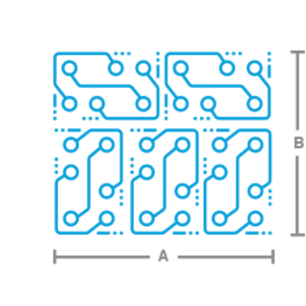

Inner layers preparation
In case the printed circuit board is made up of several layers (multilayer), each one is order following the stack-up list.
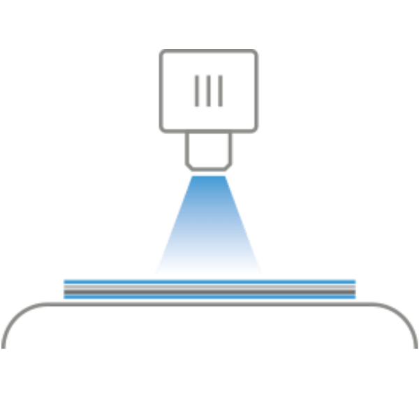
- The process always starts from a copper laminate (core), upon wich a Pre-Preg layer is applied on both sides: it is made up of glass fibers and epoxy bromine resin, used as non-conductor and adhesive between the layers.
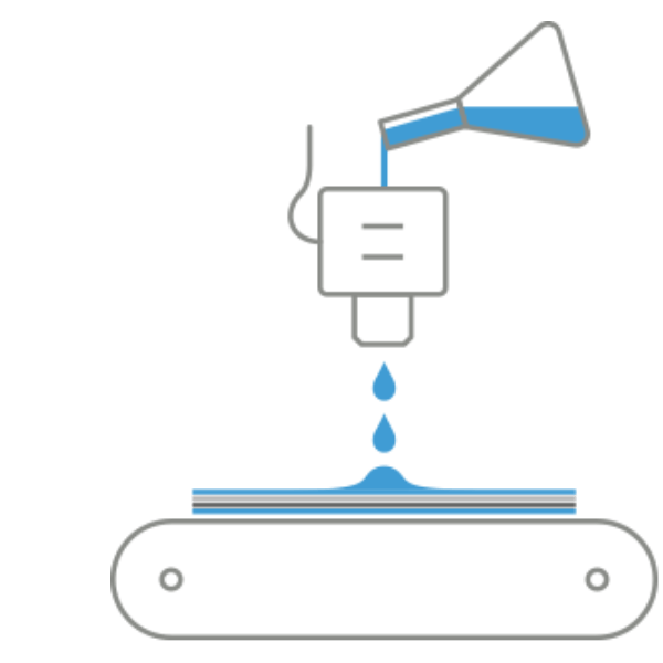
- A photographic dry film is rolled out on the copper laminate that, after being exposed to UV rays, will let the copper to only cover traces, pads and power supply areas. At every manufacturing stage a cleaning cicle is performed via caustic soda solutions.
- After copper etching, at the most fluid moment during hot pressure, copper is oxidised and resins are hold inside.
04
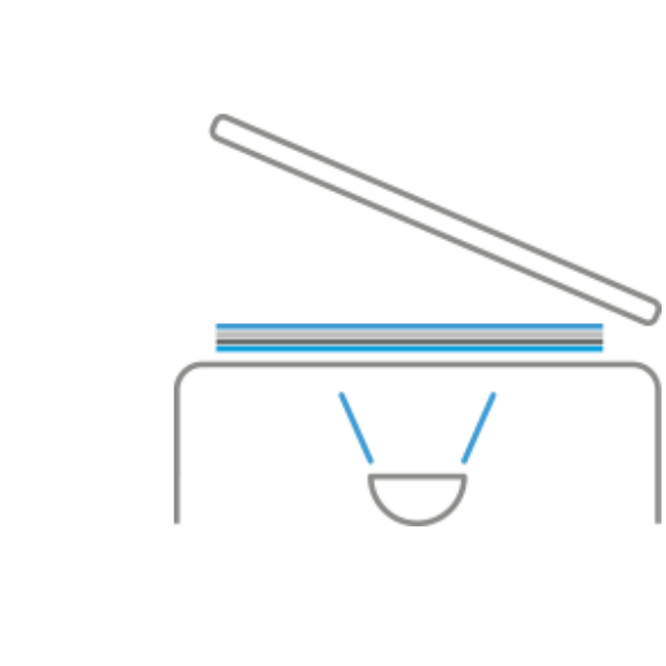
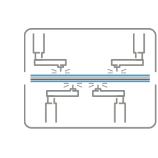
Automated Optical Inspection (AOI)
Next step is the material layup, the layers are stacked up and the outer sides are covered with a copper foil. The layers are than vacuum, high temperature and high pressure laminated: during this process, heat melts and hardens the epoxy resin and the Pre-Preg, while the pressure fuses the board in the resin. Several PCBs are laminated simultaneously, separated by dividers (metal sheets), to optimize process output. Finally, the trimming removes the flash, leaving the panel clean and ready for the next step.
05

Inner layers vacuum pressing
This is followed by the overlapping of all the inner layers, the whole is “packed,” and coated on both outer sides with a copper foil. The layers so arranged are then laminated in a vacuum, at high temperature and high pressure: during this procedure the heat melts and hardens the epoxy resin of the Pre-Preg, while the pressure engulfs the printed circuit board in the molten resin. Multiple PCBs are pressed simultaneously, separated by dividers (steel plates), to optimize the process. Final trimming removes excess material, leaving each individual PCB clean and ready for the next step.
06
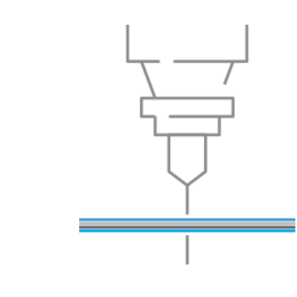
Drilling
After lamination, inner layers are fused and thus only the outer sides are visible: the PCB is now processed as if it was a simpler single face. After having identified the registry points via X-rays, PCB panels are drilled using a CNC drilling machine. It’s possible to stack-up up to three panels for a standard thickness of 1,6mm, an aluminum sheet is used as a runner and also to avoid flows, while a carboard is used at the base to protect the machinery from damages and scratches. It is critical that the drill bits used in this high-speed tool (~12.000 rpm) are constantly sharpened and serviced to gran the best precision and clear-cut in the holes. At the end of the process, the surface is cleaned using a mechanical brush, but also the holes are cleaned using oxygen plasma to remove every copper debris, granting the best electric conductivity.
07

Electroless plating
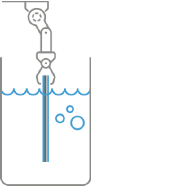
During this step, a copper conductive film 0,5-0,7 µm thick is applied, the goal is to create electrical connection between the holes and the layers. This conductive layer is needed for the subsequent process of copper plating.
08
Outer layers lamination and exposure
Just as for the internal layers, after an increase in the in pressure and temperature, the surface becomes sensitive to UV rays (photographic Dry-film). Exposure, in this case, is negative and the traces can be galvanized via copper plating, instead areas between the traces are covered via a polymerized laminate. Again, another automated optical inspection AOI is conducted to verify the outcome of the process.
09
Copper and tin plating
The electro-deposited copper is applied to all the traces and holes, granting electrical connection between the conductors on the layers. In this phase the target copper thickness is reached, it should be at least 21 microns on the inside hole surface. A second plating process is performed, the purpose is to protect the areas covered in conductive copper during the following etching phase. Often this is referred as “etching resist”.
10
Stripping and etching
After having removed the dry film from the outer surface to expose the copper, etching is conducted to leave the copper only on pads and traces covered by tin, then removed (stripping).

11
Automated Optical Inspection (AOI)
One more automated optical inspection AOI is conducted to test the outcome of the process.
12
Solder mask
Upon client request, it is possible to apply a 15-25 microns thick cover layer called solder mask. The purpose is to protect the copper surface that will not be covered during the assembly but also prevent shorts.
13
Surface Finish
To protect copper surfaces not covered by the solder mask, several finishing techniques can be employed, the most common are: Hot Air Leveling (HAL), Electroless Nickel Immersion Gold (ENIG), Hard Gold plating, etc..
14
Legend print
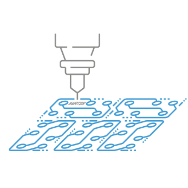
Information such as product codes, legend and other details can be printed on the PCB using a silk-screen printer.
15
Routing
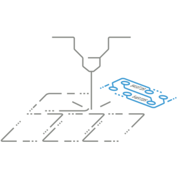
Individual PCBs are cut out from the panels using a CNC machine.
16
Electrical test
All the PCBs undergo testing to verify the overall quality of the production process. Multiple instruments are used, like flying probes and bed of nails.
17

Final quality control
After the instrumental test, the PCBs are visually inspected by the technical staff. Scratches, impurities and everything listed in the applicable IPC rules is thoroughly looked for.
18
Shipping
Aiming to reduce as much as possible the risk of PCB deterioration, in the individual thermos-shrinking blisters, silica gel and humidity indicator are always added. On the outside, an adhesive label indicating product code, quantity and data is applied. All this information will be displayed also on the outer box, granting a continuous tracking of each shipping.
